PCB Design — A Hobbyist’s Perspective

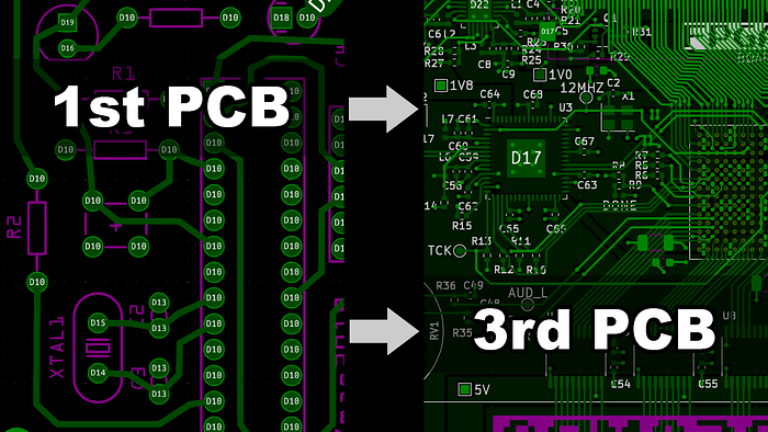
Being a software engineer by trade, I got into hardware design as a hobby a couple of years ago. By hardware I mean mostly printed circuit boards (PCBs). Having control over both hardware and software is a great way to get creative. I’ve only designed 3 boards so far yet I feel like I already learned a lot in the process. In this post I’m going to share some of the things I learned. That being said, I’m by no means an expert on PCB design nor on electrical engineering — please keep that in mind when reading this.
From Breadboard to PCB
Just like many hobbyists, I started with an Arduino and a couple of components on a breadboard. Once I had a working design, I wanted to integrate it all on one board. This meant first looking at the Arduino board and figuring out which of its components I’d need on my board, too. Then combine that with the components I had on my breadboard. Sounds easy enough and it is actually not that complicated. Since a typical Arduino doesn’t communicate with GHz speeds and it operates on a single voltage only, the actual design of your hardware is bound by few constraints only. Apart from that, the Atmega328 microcontroller of the Arduino Uno is available in a through-hole package, so your whole board can be assembled entirely by through-hole soldering which a lot of beginners tend to find easier than dealing with surface mounted parts.
I did my first board design using Fritzing but quickly moved on to Eagle and ultimately KiCad for my second and third board. KiCad is open-source and works great for simple and even more complicated hobbyist designs.
Creating a board using KiCad (or any software for that matter) typically involves the following steps:
- Drawing the schematic — this often includes drawing custom symbols and footprints for the required parts
- Laying out the design for physical production on a PCB
- Creating a bill of materials (BOM)
- Having the PCB manufactured
- Assembling the board or having it assembled
While I did assemble my first board manually, I had my third board assembled by PCBWay, who also kindly sponsored the fabrication of the board. I did this because the BOM contains a whopping 145 parts with many of them being as small as 0.6mm. PCBWay offers a great turn-key assembly service where they source all the parts and assemble the boards for you.
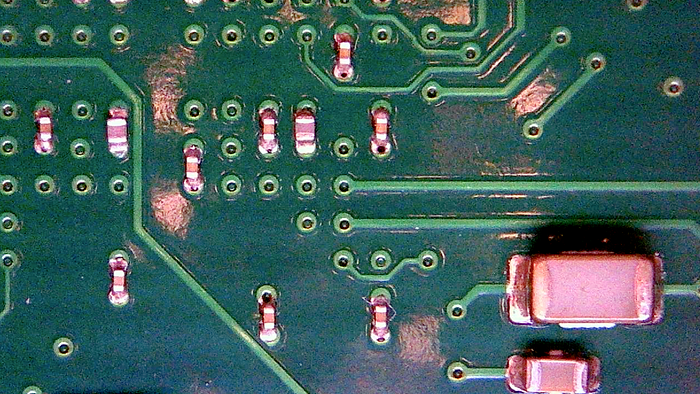
This was the first time I placed capacitors directly on top of vias on the backside of the board and I wasn’t sure whether it was going to work or not. It did work out just fine as you can see in the picture below.

If you’d rather assemble your boards yourself and still want to use surface mounted components you can do so pretty easily at home, too. I did this for my second board using tweezers, solder paste and a cheap toaster oven. That way you can do your own reflow soldering and the results are pretty good if you’re willing to put in the work.
Now, let’s have a closer look at the actual PCB design process since this is the exciting part after all.
Things to keep in mind when designing PCBs
I’m going to list a couple of things I learned to keep in mind when designing PCBs as a hobbyist. The list is in no particular order and depending on the actual project the items may be of varying significance.
Datasheets Are Your Friend
Whether you already know what components you’re going to use or you’re still trying to find the right ones, datasheets are your friend. Datasheets also tend to be these huge and daunting documents but that’s okay — there’s no need to read it all. Depending on your actual goal you’re only looking for a specific section of the datasheet. When trying to find a suitable component, look at the summary at the top of the datasheet. When designing the circuit, look at reference designs and typical applications in the datasheet. When designing your PCB, look at the footprint section of the datasheet. Most of the time, that’s all you need.
The Obligatory Decoupling
This is something people will tell you over and over again and it may easily get overlooked by beginners: All digital and probably most analog ICs needs decoupling from the power source. In simple cases this just means placing a 100nF capacitor as close as possible to the IC’s power input. In more complex cases (e.g. with BGAs) entire networks of decoupling capacitors are required. As always, you can find the necessary information in the chip’s datasheet.
Btw, the picture above shows some of the decoupling capacitors for a single BGA IC.
4 Layers vs. 2 Layers
In terms of hobby designs you can usually achieve a lot with 2 layer PCBs. There are still many good reasons to switch to 4 layers for all but the most simple designs, however. With 4 layers you typically have two signal layers — one at the top and one at the bottom of your PCB — and one of the inner layers dedicated to a ground plane and the other one to a power plane. If required the power plane may be split up into multiple voltage domains.
Compared to a two layer design, this setup simplifies routing because you don’t need to worry about routing your power rails. You’ve got access to the power supply everywhere on your board through vias. On top of that, power and ground planes offer improved signal integrity by optimizing current return paths (see also the next section) as well as additional capacitance (a power plane and a ground plane separated by a dielectric is basically a capacitor).
Return Paths
This is one of the harder concepts to wrap my head around and it only really matters for high speed signals. That being said, high speed doesn’t necessarily mean digital signals in the GHz domain. High speed means rapidly changing signals and a 1 kHz signal can very well be high speed if its raising and falling edges (the change from high to low and low to high) are rapid enough — which is more or less the case with modern ICs anyway. The good news is that if you’re doing a 4 layer design and you route your high speed signals on top of a suitable reference plane (GND is always suitable) then you’ve got your return paths under control. That’s one of the reasons I like doing 4 layer designs. Otherwise you’d need to put more thought into where your return paths are.
Real Estate Is Plentiful
I see this with a lot of boards designed by beginners and I’m guilty of this, too: We tend to spread out our components too generously, leaving a lot of empty board space in between and drawing unnecessarily long traces. Things can be packed up a lot more tidy than you’d think. Of course, if you plan to solder manually or you’re expecting to do a lot of rework, having space to work with is actually benefitial.
Route Important Signals First
When you’ve finished your schematic and you’ve done a rudimentary placement of your components on the PCB, route the most important signals first (e.g. clock signals or communication buses). These signals are the ones most likely to be affected by poor signal integrity and can benefit a lot from having put more thought into their layout. This means keeping the distances short, not using too many vias, and have their return paths under control. Apart from high speed digital signals, analog signals can also be vulnerable to interference.
Trace Width vs. Trace Spacing
How wide does a trace have to be and how far apart should traces be from each other? Well, these questions are partly answered by the manufacturer of your PCB. They will give you a minimal trace width and a minimal trace spacing they can work with. That being said, it’s seldom a good idea to design at the limits of what your manufacturer is capable of.
I’ve seen different opinions on trace widths. Some recommend to have traces as wide as possible to lower their resistance. Then again, wider traces mean less space in between which can cause cross-talk between different signals. As I understand, there are a lot of things to consider when deciding on how exactly your traces are going to look like. Most of it probably doesn’t matter that much for hobbyist boards, anyway. One thing to keep in mind, though: Make sure your traces can handle the amount of current you’re going to put through them. There are free calculators out there to help you calculate trace widths based on current requirements.
Test Points
Adding test points to your PCB isn’t required but it can make your life a lot easier. A test point is usually just a bit of exposed copper (i.e. an unused pad) that gives you quick and easy access to probe signals with your oscilloscope or your multimeter. Make sure to also expose a couple of GND points for reference. I always add test points to every voltage domain to check whether the voltages are correct and stable. On top of this, I usually add test points to clock signals and communication buses. It’s up to you to decide how far you want to go with this — just make sure to give it some thought before sending your design off to be fabricated.
Final thoughts
I’ve not given you a cookbook recipe for PCB design as this would be hard to do anyway, and it would neglect a lot of the creativity you need to put into your own designs.
I still hope the points listed above provide you with enough food for thought for your own hardware endeavors. I also suggest doing more research on the topics you’re most interested in. If you’d like to know more about signal integrity and PCB design in general I highly recommend this YouTube channel.
Also, let me know if you think I missed something important or if I made a mistake.
