Memory and Memory-Mapped I/O of the Gameboy — Part 3 of a Series

In the second part of this series I was talking about the Gameboy’s CPU and how it can be emulated. The DMG CPU’s contact to the outside world is through memory and memory alone — at least that’s what it looks like to the CPU itself. Some of the memory is actually peripherals in disguise. I’m about to explore what this means.
The Address Bus
When I say memory I actually mean the address bus. As discussed in a previous post, the DMG CPU uses 16 bits to address contents in memory. The program counter (PC) uses 16 bits to fetch instructions from memory and the stack pointer (SP) uses 16 bits to point to a location in memory. On top of that, a lot of instructions take arguments to read from or write to locations in memory — each of them addressed by 16 bits.
That’s the only access to the outside world for the CPU. Every time the CPU wants to access something other than its internal registers, it has to use the address bus. And the only operations possible on the address bus are read and write. That’s why I say everything looks like memory to the CPU — it might as well be all memory, the CPU wouldn’t be able to tell the difference.
Memory-Mapped IO
If it’s not all memory, what else is on the address bus? The answer is: basically everything else. The video controller, the sound controller, the buttons, the cartridge — they’re all on the address bus.
Now, I haven’t done much research in terms of the actual hardware of the Gameboy since, for an emulator, the only relevant information is where inside the address space each of these peripherals is located and how they’re supposed to behave.
The 16 bits of the address bus can be used to address up to 2¹⁶ bytes which may sound like a lot yet is actually only 64 Kilobytes. Each peripheral gets a dedicated region or location inside this 64 kB address space. For example: the master switch for the sound controller (sound on/off) is located at the address 0xFF26. If the CPU wants to turn the audio on or off it has to write to this exact location on the address bus. I want to emphasize that it makes no difference to the CPU whether it’s writing to this specific location or any other location in memory. In fact, the CPU has no concept of a sound controller at all. It’s just the developer of the currently running code who’s instructing the CPU to write to this location. To the CPU it’s all just writing and reading on the address bus. Some of the writing operations may put images on the screen, some may control sound output while others just write bytes into RAM.
Memory Map of the Gameboy
The 64 kB address space of the Gameboy can be separated into 12 regions:

Let’s have a look at each one of these regions, starting at the bottom.
ROM and Switchable ROM Bank
The first two regions contain 32 kB of address space and are mapped directly to the cartridge. This is where the actual game is stored and it takes up half of the available address space. For some games like Tetris these 32 kB are enough but others like Super Mario Land need more space. This is where switchable ROM banks come into play. A Gameboy cartridge may contain more than 32 kB of ROM. By writing to specific registers of the memory bank controller in the cartridge (also located on the address bus) the upper 16 kB of ROM space can be mapped to different physical ROM locations.
As my goal for now is to just run Tetris, I’m not going to implement switchable ROM banks just yet.
Video RAM
The Gameboy’s Video RAM starts at location 0x8000 and contains up to 8 kB of tile data. For performance reasons pixels cannot be manipulated individually by the program. Only tiles of 8x8 pixels can be placed on the screen. Tiles can be part of the background map or they can be part of sprites. If you’d like to know more about how exactly tile data is stored and accessed inside the Video RAM I encourage you to read the corresponding parts of the Pan Docs — a documentation every Gameboy developer should know well.
Switchable RAM Bank
A cartridge may include additional hardware RAM. Starting at 0xA000 8kB of address space on the bus is reserved for this. By switching RAM banks cartridges can provide up to 32 kB of additional RAM. Just like switchable ROM banks, I won’t be implementing this for the first prototype of my handheld console.
Internal RAM
Located at 0xC000 on the address bus is the beginning of 8 kB of internal RAM. This is just bytes that can be written and read by the CPU. This is trivial to implement for en emulator as it is just an array of 8 bit integers.
Sprite Attributes
This is the part of the memory where sprites are defined. It references the tiles inside the Video RAM. The display controller is able to display up to 40 sprites per frame with a limitation to 10 sprites per line. A sprite is composed of either one or two tiles and its size is either 8x8 or 8x16 pixels. Each byte inside the Sprite Attributes Memory contains the description for one sprite. This description includes the sprite’s tile number, its x and y position on the screen, the information on whether it should be displayed flipped horizontally or vertically, as well as information on its color palette (the color palettes are defined in the I/O region on the address bus).
I/O
The I/O region of the address bus is connected to a lot of peripherals:
- Video Controller
- Sound Controller
- D-Pad and Button Inputs
- Serial Data Transfer via Link Cable
- Timer
For now, I’ll just be implementing parts of the video controller. No sound yet, no button inputs, no serial data connection and no timer.
I’ll be talking about the video controller in more detail in my next post.
High RAM
High RAM (HRAM) is an area of RAM that can be accessed very quickly and it’s also the only part of memory that accessible by the CPU during a DMA update of the Sprite Attributes Memory, a method of updating the sprite attributes without consuming CPU cycles. I’ll be revisiting this concept when implementing the video controller.
Interrupt Register
I’ve mentioned interrupts a few times now and I’m going to explain what they are in the next section. The Interrupt Register is just an 8 bit value consisting of flags (single bits) to indicate what kind of interrupts are enabled. This can be controlled by writing to the location 0xFFFF on the address bus.
And now let’s talk about interrupts.
Interrupts
Understanding the basic concept of interrupts is pretty straight forward: they interrupt the current program flow in response to certain events.
What does this mean? We’ve seen that the CPU just executes whatever instruction the program counter (PC) points at. The counter is automatically incremented and it can be altered by certain instructions. That’s all about how a program is executed — except for interrupts. When an interrupt occurs, the current program counter is pushed onto the stack and a new value for the PC is set according to the interrupt. Each interrupt has its own specific starting point in memory. For example: when a button is pressed, an interrupt is requested and the PC is set to 0x0060, meaning the program continues its execution at this location. At the end of whatever code there is, a return from interrupt instruction is meant to be called which pops the original PC from the stack and continues the ordinary program flow.
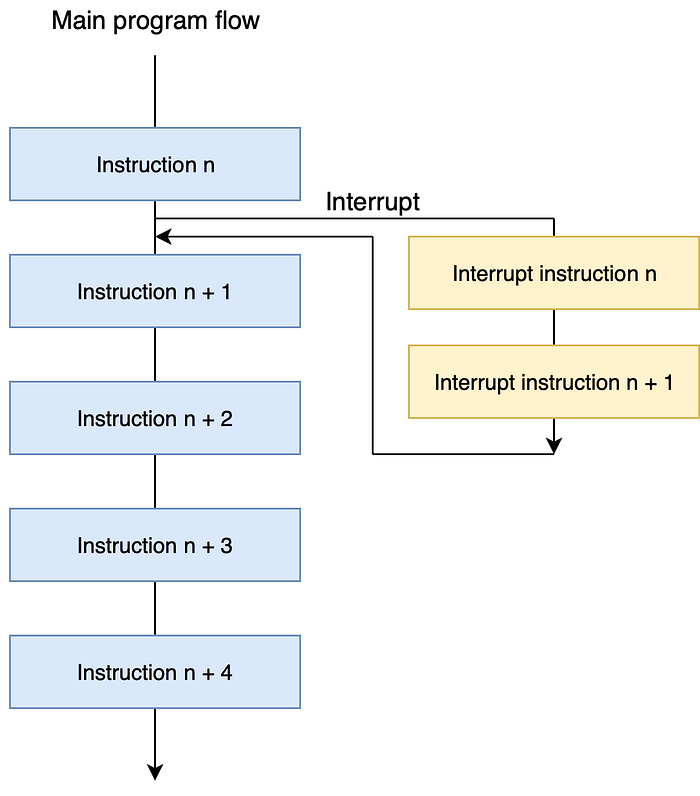
The button interrupt isn’t a good example, however, as it’s rarely used. Button states are usually read once per frame — which brings us to another, very important interrupt: the vertical blank interrupt. This interrupt is requested by the video controller and it occurs at the end of each full redraw of the display and therefor about 60 times a second. Game developers may think of this as the main loop to read the current state of the buttons and generate a new frame. This is the most important interrupt for me to implement in order to run Tetris.
To summarize: The main program flow is interrupted 60 times a second to indicate that a frame has been fully rendered and a new one may be generated next.
Besides the vertical blank interrupt and the button interrupt there are a few other display-related interrupts as well as a timer interrupt and an interrupt for serial data transfer.
This has been a very high level overview of the Gameboy’s memory mapping and it’s by no means meant as a complete description of the topics discussed. If you want to know more I highly recommend the already cited Pan Docs as well as other great resources that are out there. As I’ll be building hardware, too, I cannot focus on writing the emulator alone. That’s why my first goal is to run Tetris, wich will be done with my next post, and then I’ll be focussing on the hardware for a while. This also means that future posts may get more practical compared to these last two highly theoretical ones.
The Series so Far
Part 1 — Building a Gameboy From Scratch
Part 2 — The CPU
This— Memory and Memory-Mapped I/O
Part 4 — Running Tetris
Part 5— Display Timing Circuit
Part 6 — Behold the Breadboard Gameboy